


1. Introduction
For U.S. Department of Defense (DoD) directed-energy applications, nonintrusive electric and magnetic field probes can solve several technical problems associated with conventional probes. Conventional sensors perturb the field. They could be used for tests and evaluations (T&Es) if the T&E tolerates such field perturbations. But in a complex test environment, they are not suitable because the sensor’s field perturbation produces irreproducible and inconsistent test results. Other problems, such as limited bandwidth and dynamic range and metallic cables, make the conventional sensors difficult or impossible to use for many critical tasks. To overcome these problems, we developed a nonintrusive electric field sensor, which is made of all-dielectric materials. It negligibly perturbs the field that it measures. The sensor has an extreme dynamic range and nearly flat frequency response over the frequency range from 0 to 20 GHz. Its vector field detection capability enables us to measure the strength and direction of a radio frequency (RF) field simultaneously, fulfilling the DoD requirements for various high-power microwaves (HPMs), high-power RF (HPRF), and electromagnetic (EM) pulse applications (EMP).
Presently, D-dot and B-dot sensors and some diode sensors are widely used for various electromagnetic T&E. These sensors contain metallic components and typically use electric cables. They may be suitable for simple T&E tasks. However, in a complex test environment, they are not acceptable for subtle investigation of EM field interactions since the sensors and cables themselves perturb and distort the EM fields. Also, as their frequency bandwidth is limited, they are often unable to replicate the complex EM waveform (e.g., short pulse), which contains a wide range of Fourier frequency components. In addition, their limited dynamic range and signal degradation in the coaxial cable cause many technical challenges. Because of these disadvantages, it is very difficult or impossible to perform certain T&E with conventional sensors.
As an alternative, a nonintrusive electric field sensor made of all-dielectric materials can solve the problems mentioned [1–7]. We constructed a nonintrusive sensor and demonstrated that the sensor negligibly perturbs the field that it measures [1]. Its frequency range is from 0 to 20 GHz, with a dynamic range from 0.1 to 1 V/m up to 500 kV/m. As it can detect all Fourier components over a wide range of frequency, the sensor detects and replicates a complex waveform. The sensor is suitable to perform all different types of T&E, even in a very complex test environment.
2. Naval Research Laboratory (NRL) Electro-Optic (EO) Field Sensor Principle
The NRL EO sensor is made of a KD*P crystal to prevent problems associated with photorefraction and other materials’ problems [9–11]. When a KD*P crystal is grown, it has a characteristic crystal shape, as shown in Figure 1 (A). Conventionally, the crystal’s lattice directions, <100>, <010>, and <001>, are assigned as x-, y-, and z-axes, respectively.
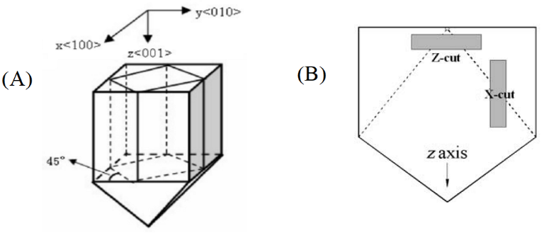
Figure 1: (A) The Crystal Axes of a KD*P Crystal and (B) the Definition of Z- or X-Cut KD*P Crystal (Source: NRL Data).
The KD*P crystal is a birefringent material and has the ordinary refractive index no in the x- and y-axes and extraordinary refractive index ne in the z-axis, with corresponding values about 1.4948 and 1.4554 at the probe beam wavelength of 1.06 mm. The values of no and ne are dependent on the wavelength as well as on the probe beam direction with respect to the crystal’s lattice (Figure 2). If it travels in a tilted direction z’, the refractive index is in between ne and no, depending on the angle θ [5].
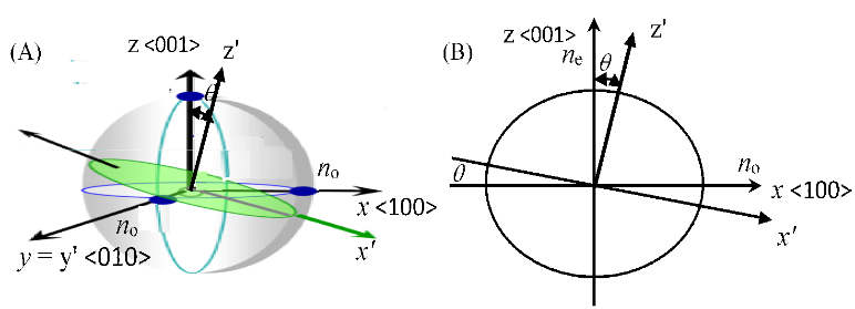
Figure 2: (A) The KD*P Crystal’s Lattice Directions and Corresponding Refractive Indices in a 3-D Presentation and (B) the Refractive Index in the x-z Plane (Source: NRL Data).
Figure 3 shows the schematics of our single-axis EO sensor that uses an x-cut KD*P crystal, and Figure 4 shows the retardation between the optical field components Ex‘ and Ey‘ of the probe beam that results in the polarization rotation of the probe beam. Its z-axis is slightly tilted against the probe beam’s direction. The polarizer ensures the probe beam’s polarization direction to be θ1 = 45°, leading to the same amount of the vertical (x-direction) and horizontal (y-direction) optical-field components.
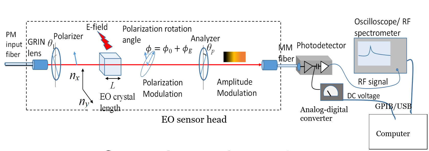
Figure 3: A Schematic Diagram of an NRL Single-Axis EO Field Sensor. The Dashed Rectangle Box Indicates the EO Sensor Head (Source: NRL Data).
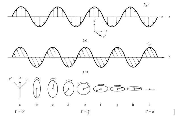
Figure 4: (a) Two Optical Field Components (Ex’ and Ey’) in the EO Crystal and (b) the Combination of Ex’ and Ey’ Determines the Polarization Direction of the Probe Beam, Which Changes From Linear Polarization to Elliptical to Circular to Elliptical and Then to Linear, as the Probe Beam Traverses the EO Crystal (Source: NRL Data).
When exposed to an external E-field, the E-field alters the crystal’s refractive indices nx and ny to n‘x = c/v‘x and n‘y = c/v’y, since n = c/v, where c and v are the speeds of light in vacuum and a medium, respectively. Here, we assume that an external E-field is applied to the z-direction and that the crystal’s x-axis is approximately aligned to the optical field component Ex’. If the external E-field in the z-direction ![]() , the altered refractive indices can be expressed as
, the altered refractive indices can be expressed as
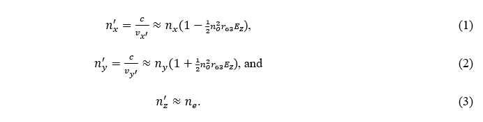
Here, r63 is the EO tensor of the crystal.
As vx‘ ≠ vy‘, it results in the polarization rotation f of the probe laser beam.

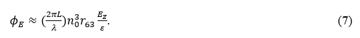
The electric field is applied to a dielectric medium. So, we should consider the electric displacement field Dz. Since D = εE, where ε is the dielectric function, Ez = Dz in free space, but the E-field becomes Dz/ε inside a dielectric medium. In other words, Ez changes to Ez/ε inside the dielectric. So, we replace Equation (4) with the following:
![]()
The first term in Equation (5) is the natural polarization rotation. As illustrated in Figure 2, the crystal is tilted so that nx ≠ ny and, consequently, ø0 ≠ 0.

The second term in Equation (5) is the polarization rotation created by the EO effect.
After passing through the EO crystal, the probe beam’s polarization direction is θ1 + ø. The initial intensity of the probe beam is I0, and the polarization direction of the analyzer is set to be θp. After passing through the analyzer, the beam intensity will become I = I0cos2(θ1 + ∅ – θp). The photodetector’s signal voltage can be expressed as
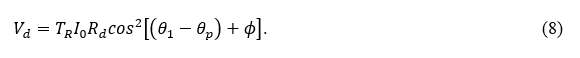
Here, Rd and TR are the photodetector’s responsivity and the EO sensor head’s transmissivity, respectively. In the sensor, we set ![]() . Assuming ΦE is small, we can rewrite Equation (8) as
. Assuming ΦE is small, we can rewrite Equation (8) as

The first two terms on the right-hand side correspond to an optical beam output that generates a DC voltage from the photodetector.
The third term in Equation (9) is the EO modulation signal.
![]()
Figure 5 shows the EO polarization rotation ∅E and the sin∅E as a function of Ez by assuming the following parameter values: L = 14 mm, λ = 1550 nm, n0=1.4931, r63= 24×10-12 m/V, and ε = 3. If ΦE is not too large , we can assume sinΦE ≈ kΦE, where k is a coefficient. Then, Equation (11) can be rewritten as follows:

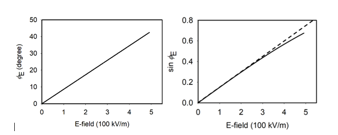
Figure 5: (Left) The EO Induced Polarization Rotation Angle ΦE vs. E-Field Applied to the EO Crystal and (Right) sinΦ as a Function of the E-Field (Note the Sine Function Is Almost Linear Until E ≈ 300 kV/m) (Source: NRL Calculations).
From Equations (11) or (12), the E-field Ez can be assessed from the measured EO signal strength VEO, providing that the parameter values of L, λ, Tr, I0, Rd, Φ0, no, r63, and ε are known and do not vary. However, in reality, these parameters—especially the probe beam intensity I0—vary over time.
From Equations (10) and (11), we could derive Equation (13), which indicates that the EO signal strength VEO changes nonlinearly with the initial probe beam intensity I0.

Figure 6 shows such a probe beam intensity dependence obtained from an NRL single-axis EO sensor. The dots are experimental data, and the solid line is a theoretical curve. Because of this probe beam’s intensity dependence, if we measure Ez only based on the EO signal VEO, we should employ a very stable and robust probe laser, which is often hard to achieve in reality.
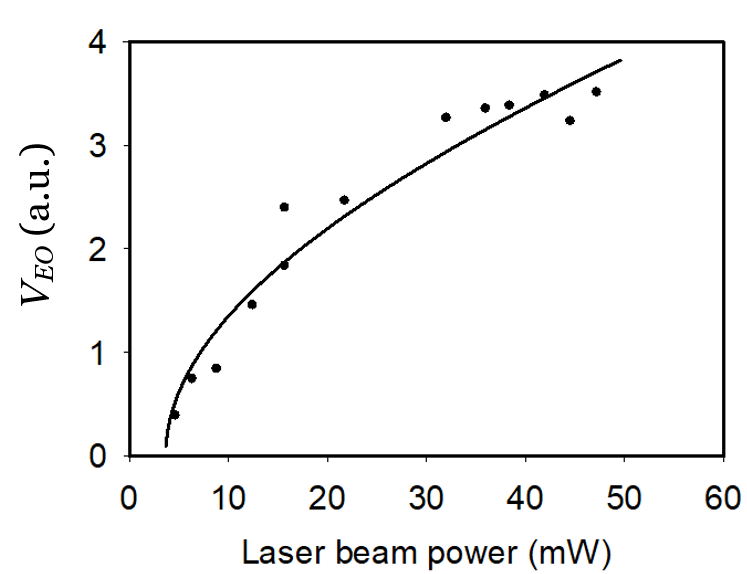
Figure 6: An NRL EO Sensor’s Signal Strength VEO as a Function of the Laser Probe Beam Power (Source: NRL Data).
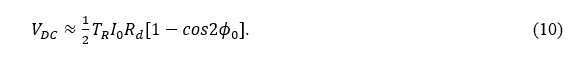
To circumvent this problem, instead of relying only on the photodetector signal VEO, we alternatively measure an EO modulation depth mEO. We can obtain the following equation from Equations (10) and (11) [6, 8]:

Assuming sinΦE ≈ kΦE, Equation (14) can be rewritten as
![]()
The value of the coefficient K can be obtained from the parameter values of L, λ, ϕ0, k, no, r63, and ε, or more conveniently K(≈∆mEO/∆Ez) from the measurement of mEO as a function of Ez, through the sensor calibration procedures. Then the field strength Ez can be extracted from the following relation:
![]()
We define Cf = 1/K as a conversion factor for a given EO sensor. Equation (16) implies that the smaller the conversion factor, the higher the EO responsivity.
Figure 7 shows two examples of the sensor calibration data taken from the same EO sensor, measured with either a 1-GHz continuous wave (CW) RF signal or an RF pulse in a transverse electromagnetic (TEM) cell. The RF pulse width was about 5 ns, and its pulse repetition rate was 1 kHz. From these data, we extracted a conversion factor Cf = 478 for the 1-GHz CW RF field and Cf = 9476 for the pulsed RF field. This suggests that the EO sensor is much more responsive to the CW RF field because the effective dielectric function e of the EO crystal depends on the RF signal type. We found similar behavior from the D-dot sensor.
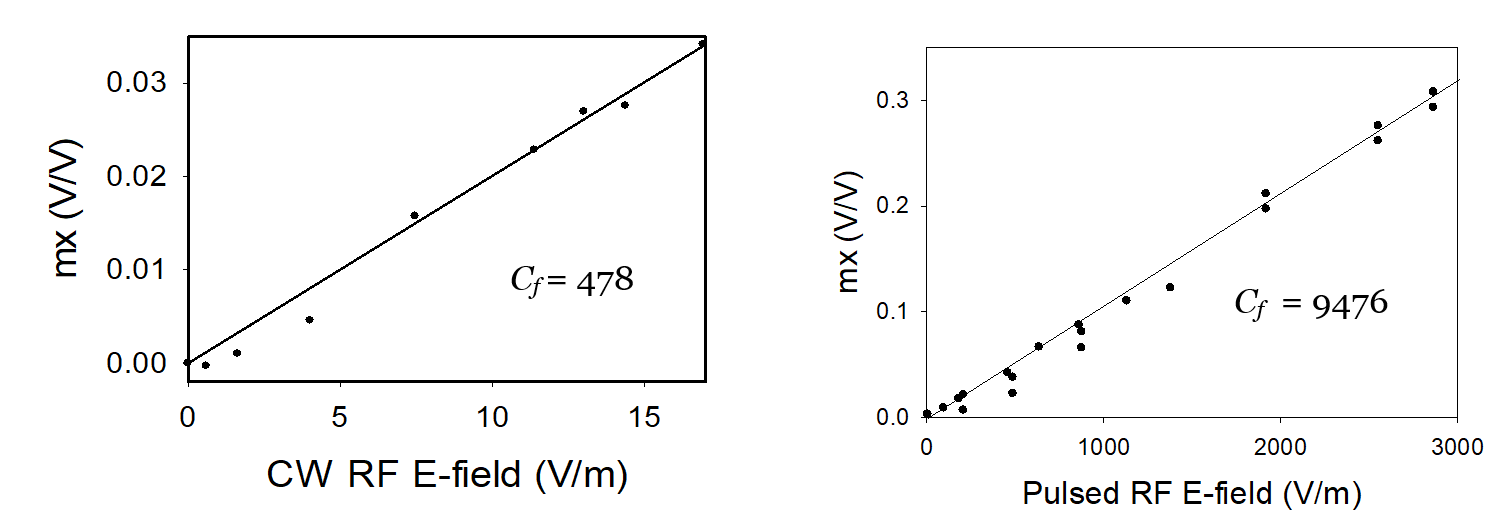
Figure 7: The EO Modulation Depth vs. a 1-GHz CW RF Field (Left) and a Pulsed RF Field (Right) From the
Same NRL Single-Axis EO Sensor (Source: NRL Data).
3. Comparison Between the D-dot and EO Sensors
We compared one of our single-axis EO sensors with a D-dot sensor (Prodyn Model AD-70D with a Balun Model BIB-100F), which has a 3-dB bandwidth over the 200-kHz–3.5-GHz frequencies. We characterized the sensors in a TEM cell (Figure 8). The D-dot sensor contains a dielectric material whose relative permittivity varies with the RF frequency. Over the 100-MHz–1-GHz frequency range, the D-dot sensor’s responsivity changes nearly three folds. In contrast, the EO sensor’s responsivity was nearly flat (responsivity variation <50%).
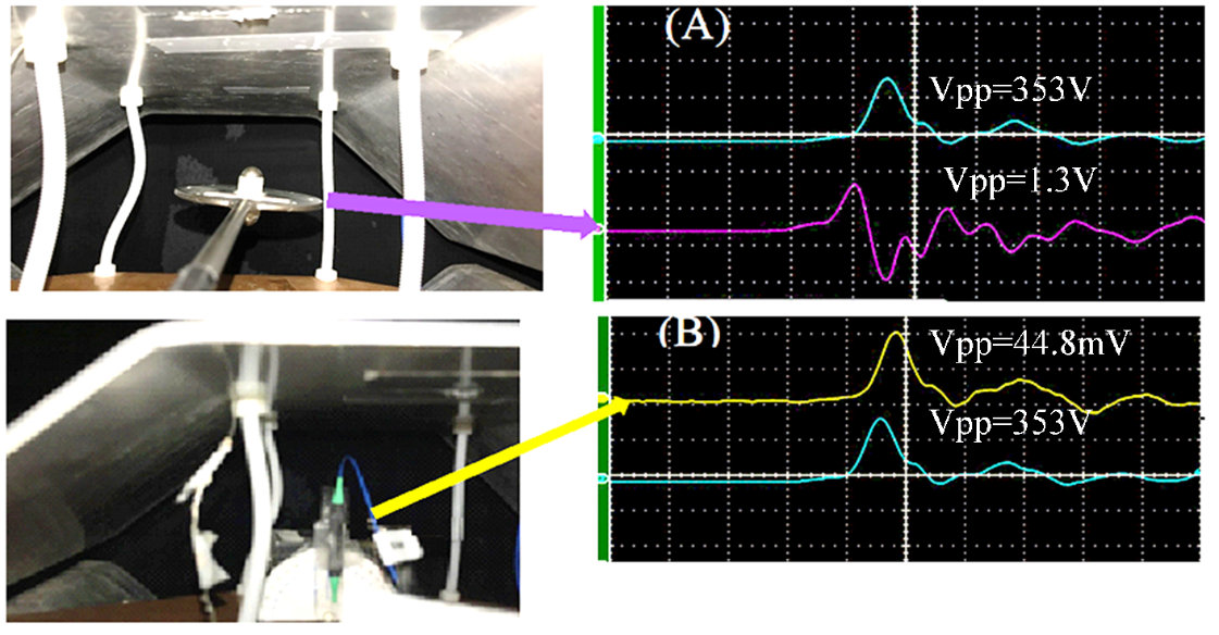
Figure 8: (A) A D-dot Sensor in the TEM Cell Generated a Peak-to-Peak Voltage of 1.3 V (Bottom Trace) When a 353 V, 5-ns Pulse (Top Trace) Was Applied to the TEM Cell. (B) A Similar Setting With a Single-Axis EO Sensor Yielded a 44.8-mV EO Signal (Waveform Shown on the Top Trace) (Source: NRL Data).
The D-dot sensor measures the time derivative of an RF waveform. If the D-dot signal is integrated, one may, in theory, recover the original RF waveform. But, in reality, recovering a short RF pulse by integration is not trivial. In contrast, the EO sensor duplicates the RF pulse with negligible distortion, as shown in Figure 8. But the D-dot sensor produces about 29× stronger signal than the EO sensor does for the same RF field.
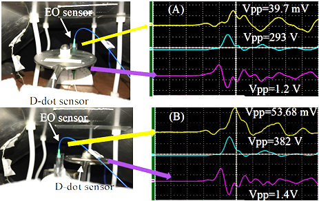
Figure 9: (A) The D-dot Sensor Placed About 2 to 3 cm Away From the EO Sensor Distorted the RF Signal Waveform and Reduced the RF Signal Strength Measured by the EO Sensor. (B) The Distance Between the Two Sensors Was About 5–6 cm, Resulting in Less Distortion of the RF Signal and Less Reduction of the RF Signal (Source: NRL Data).
When we placed the D-dot sensor near the EO sensor, it significantly distorted the RF waveform, which the EO sensor detected. This distortion occurs because the D-dot sensor contains metallic components that alter the E-field; the closer the two, the stronger the distortion.
4. Directional Dependence of the Single-Axis EO Sensor
If an RF field enters the crystal at an angle Φ, (Figure 10) Equation (15) can be rewritten as
![]()
The single-axis EO sensor’s output is dependent not only on the strength of ERF but also on the direction of ERF. Figures 11 and 12 show such RF field directional dependence. Because of this directional dependence, if one uses a single-axis EO sensor for a T&E, the sensor should be tightly aligned to be parallel to an incoming RF or microwave signal. Such a requirement is difficult or sometimes impossible to achieve in an actual T&E environment because of the RF beam reflection and scattering in the field test.
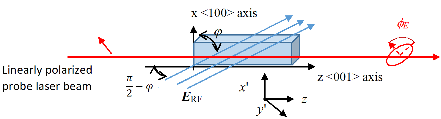
Figure 10: A KD*P Crystal With an E-field Entering at an Angle φ Against the Crystal’s x-Axis (Source: NRL Data).
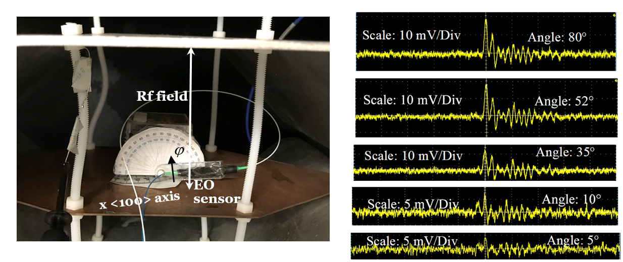
Figure 11: The RF Field Directional Dependence: (Left) The Angle φ Is Between the x-Axis of the EO Crystal and the RF Field Direction
and (Right) EO Signal as a Function of the Angle φ (Source: NRL Data).
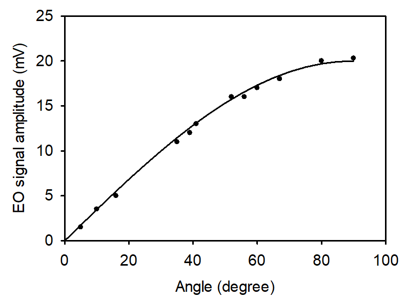
Figure 12: EO Signal Amplitude vs. the RF Incident Angle φ as Defined in Figures 10 and 11 (Source: NRL Data).
5. Three-Axis EO Sensor Prototype
To address the directional dependence problem, we instead exploited this directional dependence of the EO sensor and constructed a three-axis EO sensor prototype. The prototype consists of three single-axis EO sensors, with each sensor’s <001> axis aligned to the spatial x-, y-, and z-coordinates, as shown in Figure 13.
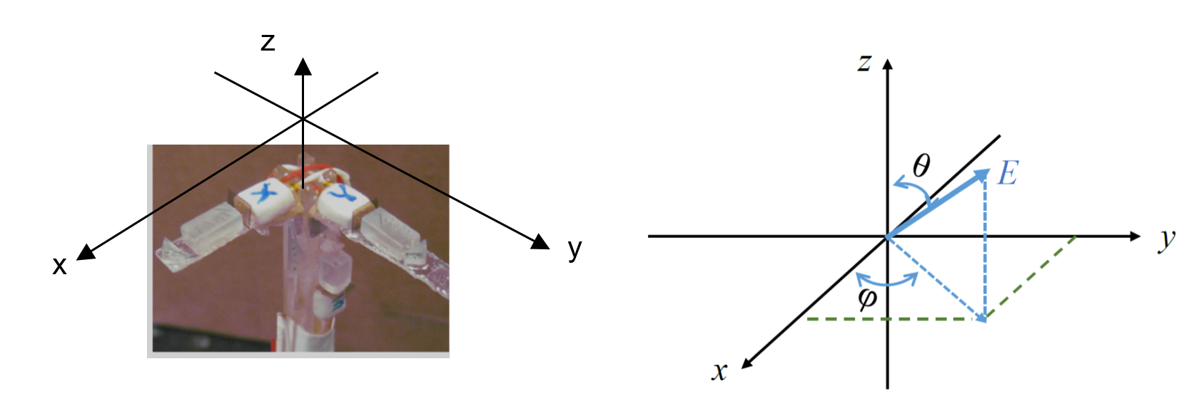
Figure 13: (Left) A Three-Axis EO Sensor and (Right) an External E-Field Applied to the Three-Axis EO Sensor in an Arbitrary Direction (Source: NRL Data).
When an E-field is applied to the three-axis sensor in an arbitrary direction, the E-field components can be expressed as
![]()
and the EO modulation depth for each single-axis EO sensor on the x-, y-, or z-axis is given as
![]()
The modulation depth coefficients can be obtained through the calibration process. The total E-field can now be determined without concerning the
E-field incident angle.
![]()
At the same time, the direction of the incident E-field is conveniently determined as
![]()
where , i ̂, j ̂, and k ̂ are the unit vectors in the x-, y-, and z-directions.
Through the calibration process with a pulsed RF field, we found that the sensors on the x- and y-axes had a conversion factor of about 25000 for a pulsed RF beam, and the one on the z-axis had a conversion factor of 42000. (The z-axis sensor is poorer than the others. We will replace it with a better one later.) Figure 14 shows the three-axis sensor mounted in a TEM cell for characterization, slightly tilted so that the RF field entered at θ= 73.3° and φ= 8.8°. The EO signal VEO and the DC voltage VDC are collected by an EO data acquisition software, which we developed. The software calculates the RF field components and the total RF field strength, as well as the field direction. It then displays the waveforms and strength of Ex, Ey, and Ez, as well as the field direction in a three-dimensional graphic on the computer screen (Figure 15). The data indicated that the RF field strength was 7080 V/m, which was correct, and its incident angles were θ = 73.3° and φ = 8.82°, consistent with the values mentioned.
Figure 14: A Three-Axis EO Sensor Mounted in a TEM Cell (Source: NRL Data).
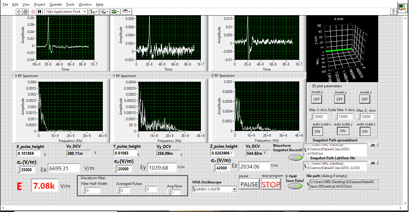
Figure 15: Screen Capture of an EO Data Acquisition Software Graphical User Interface (Source: NRL Data).
Recently, we used the same three-axis EO sensor to perform field tests in a test site and characterized an RF pulse, ranging from a few kilovolts/meter to exceeding 100 kV/m. It demonstrated that the three-axis sensor is ready for actual field tests.
6. Conclusions
By exploiting the Pockels effect, we developed a nonintrusive, three-axis EO field sensor. We demonstrated a noninvasive RF signal characterization for the frequency range from 0 to 20 GHz and over the RF field strength from 1 V/m to exceeding 100 kV/m. The NRL three-axis sensor technology is deployable for field tests.
7. Future Work/Acknowledgments
We will construct more sensors and test the sensors in various field test environments. This work has been supported by the Office of the Secretary of Defense, Test Resource Management Center, U.S. Naval Air Warfare Center Weapons Division China Lake, and the Defense Threat Reduction Agency Research and Development Directorate.
References
- Schultz, M., R. Selfridge, S. Chadderdon, D. Perry, and N. Stan. “Non-Intrusive Electric Field Sensing.” Proc. SPIE 9062, Smart Sensor Phenomena, Technology, Networks, and Systems Integration 2014, 90620H, 10 April 2014.
- Feynman, R. “QED: The Strange Theory of Light and Matter.” Guildford: Princeton University Press, 1985.
- Tsuchiya, M., T. Shiozawa, and S. Harakawa. “Electric Field Sensing and Imaging by Non-invasive Parallel-Plate Sensor.” IEICE Electronics Express, vol. 11, no. 18, 2014.
- Warzecha, A., M. Bernier, G. Gaborit, L. Duvillaret, J.-L. Lasserre. “Electro-optic Sensors Dedicated to Non-invasive Electric Field Characterization.” SPIE 7389, Optical Measurement Systems for Industrial Inspection VI, no. 738922, 17 June 2009.
- Garzarella, A., S. B. Qadri, and D. H. Wu. “Optimal Electro-optic Sensor Configuration for Phase Noise Limited, Remote Field Sensing Applications.” Phys. Lett, vol. 94, no. 221113, 2009.
- Garzarella, A., S. B. Qadri, and D. H. Wu. “Effects of Crystal-Induced Optical Incoherence in Electro-Optic Field Sensors.” J. of Electronic Materials, vol. 39, no. 6, 2010.
- Garzarella, A., and D. H. Wu. “Optimal Crystal Geometry and Orientation in Electric Field Sensing Using Electro-optic Sensors.” Optics Lett., 37, no. 11, pp. 2124–2126, 2012.
- Garzarella, A., S. B. Qadri, T. J. Wieting, and D. H. Wu. “Spatial and Temporal Sensitivity Variations in Photorefractive Electro-optic Field Sensors.” Phys. Lett., vol. 88, no. 141106, 2006.
- Garzarella, A., S. B. Qadri, T. J. Wieting, and D. H. Wu. “The Effects of Photorefraction on Electro-optic Field Sensors.” Appl. Phys., vol. 97, no. 113108, 2005.
- Qadri, S. B., J. A. Bellotti, A. Garzarella, T. Wieting, and D. H. Wu. “Phase Transition in Sr0.75Ba0.25NbO3 Near the Curie Temperature.” Phys. Lett., vol. 89, no. 222911, 2006.
- Qadri, S. B., J. A. Bellotti, A. Garzarella, T. Wieting, and D. H. Wu. “Anisotropic Thermal Expansion of Strontium Barium Niobate.” Phys. Lett., vol. 86, no. 251914, 2005.
Biographies
Dr. Dong Ho Wu is a research physicist at the Materials Science and Technology Division at the Naval Research Laboratory, Washington, DC, and is also an adjunct professor in the Physics Department at Temple University. Before joining the NRL, he served as a research faculty member in the Physics Department at the University of Maryland, College Park, from 1991 until 2001. For several months, he was a member of the technical staff at GTE Laboratories and a post-doctoral fellow at Northeastern University. He holds a Ph.D. in condensed matter physics from Tufts University.
Aaron Dougherty is a research engineer for the HPM group at the NRL in Washington, DC. He has spent his career in HPM source development and effects susceptibility testing. His interests include HPRF sources, machine learning and data analytics, antenna design, and RF propagation. He holds a bachelor’s degree in electrical engineering from the Pennsylvania State University, a master’s degree in electrical engineering, and a graduate certificate in data analytics from the Virginia Polytechnic Institute and State University.