


Introduction
For almost two centuries, the optical community has been using the same method of producing refractive lenses and optically transparent windows. They start with an optical blank that is cut, ground, and then polished/lapped to form the final optic. While this process is well suited to the simplest optics, those with a combination of planar and spherical curved surfaces, modern demands for high-definition optics are pushing the limitations of this centuries-old technology. Spherical lenses suffer from spherical aberration, which is a kind of blur caused by imperfect focusing.
Modern refractive lenses have aspheric surfaces to correct spherical and other aberrations in the lens system—the surface curvature is not constant across the aperture, as is the case for spherical surfaces. This is usually defined mathematically as the sum of a first-order curvature having a constant radius (i.e., a spherical surface) and a series of aspheric terms (i.e., intentional deviations from the spherical surface). The more aspheric terms in a surface, the higher order the optic. This involves more manufacturing complexity and costly modern methods of manufacture, such as computer-controlled precision polishing, single-point diamond turning (SPDT), or precision glass molding. Even these methods are somewhat limited in that they require the surfaces have rotational or translational symmetry and are not suitable for asymmetric, or freeform, surfaces. The old traditional means of producing optics cannot support the requirements for new emerging technologies that require higher resolution. These limitations are imposed by multiple factors, such as the cost for higher-order optics and the inability to improve on the existing manufacturing technology [1].
The state of the art in current lens manufacturing technology is a 7th-order lens [2]. Order of an optical lens refers to the complexity of the shape of the lens represented by a polynomial of certain order. The more complex a lens shape is, the higher the order of its aberration correction. Aberration is defined as the degradation of the performance of an optical lens, when the light from one point of an object does not converge into a single point after transmission through the lens. A higher-order aberration is the distortion acquired by a wavefront of light as it passes through the lens with irregularities or inhomogeneities of its refractive index and imperfections in its geometrical shape.
To correct these various imperfections/aberrations in the current technology, various techniques of refracting light are employed. For example, chromatic aberration, or color blur, is imparted by the dispersion or wavelength dependence of refractive index in the material. Similar to how a prism separates light into its constituent colors, a simple lens with chromatic aberration focuses light of different colors at different spots (Figure 1, left), resulting in color blur at the image plane (left inset). A common solution to this problem is the achromatic doublet, which uses two different types of glass—crown (low dispersion, positive focusing power) and flint (high dispersion, negative focusing power) to bring the primary colors into the same focus (Figure 1, right). The refracted spot size for the red-green-blue components is almost identical in size and location in the XYZ coordinate system (right inset).
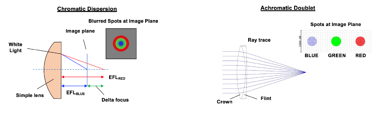
Figure 1: Chromatic Dispersion (Left) and Achromatic Doublet (Right) (Sources: J. Sugrim and D. Gibson).
This type of aberration corrections comes at cost, where different components, materials, and adhesives have to be used to bind them. The first penalty of these corrections is the reduction in optical power transmitted through the optics. The second is the size and weight. Additionally, the use of optical adhesives limits the amount optical power that the optics can transmit. Another major limitation of the current technology is that as the size of the optics grows, the fabrication of the component becomes more difficult.
Within the last decade, additive manufacturing (AM) has been successfully implemented in producing products from polymers, ceramic powders, and metals. AM is capable of producing products with intricate details on the micrometer (μm) scale. To harness the power of this new manufacturing technique, the topic “Additive Manufacturing of Inorganic Transparent Materials for Advanced Optics” was proposed and funded by the U.S. Navy Small Business Innovation Research/Small Business Technology Transfer (SBIR/STTR) Office to address the current limitation of processing optical components [1].
The sweeping intentions of this AM topic are twofold. One is to develop a technique to perform front surface repair on existing optical components.The other is to develop a manufacturing technique for producing high-definition optical components that can get beyond the 7th-order limitation of current technology. The combined goal is to produce self-contained solutions that can solve the Navy’s needs of extending the life of existing optical products and rapidly develop new optical components with higher fidelity in controlling the optical wavefronts.
Naval air operations have a broad array of weapon and surveillance systems that utilize high-performance optics. Many of these applications require greater wavelength transmission range, hardness, and temperature stability. The ability to print glass lenses using AM will provide the Navy the ability to (1) deposit net-shape or near net-shape, free-form optics; (2) locally adjust the index of refraction and other optical properties, such as dispersion; (3) create high-precision, low-thermal expansion meteorological frames which can form the basis for refractive optics; and (4) repair existing optical systems [1].
The benefits of AM are widely realized for structural systems. However, the work on printing optical components is still in its comparative nascency. The majority of the AM effort in optics has primarily focused on polymers. Processes that have been demonstrated for printing optically-transparent polymers include inkjet printing [3] with/without in-situ ultraviolet (UV) curing [4] and multiphoton stereolithography to directly polymerize resin [5, 6]. These techniques have been used for rapid prototyping of nonimaging optics using polymethyl methacrylate and similar plastics [5].
This inorganic AM topic uses a 3-inch achromatic lens as its demonstration vehicle for producing an AM process that can be used to manufacture an array of naval optical components with varying geometries. Demonstration of the AM process should include the effectiveness of fabricating fully-densified optical components with precision control of the component’s geometry and smooth surface quality. One of the key metrics that will be used to track the progress of different AM processes is the variation in the index across the surface [dn/dx] of the lens. Additionally, standard optical metrological processes will be used to examine the finished achromat lens [1].
AM for Repairs and Refurbishment in the Field
In order to extend the life of deployed, fielded instruments, an AM process is needed to repair damages to the frontoptics of these systems. Damages to these optical systems could be scratches, fractured windows, pitting, etc., to the front surface optics. These damages are most prevalent in instruments used by dismounted Warfighters exposed to harsh environments. Instrument reliability and replacement costs are issues commonly raised by product managers of Soldier-borne systems. Additionally, complex optical systems installed on ground-based mobile platforms, surface and subsurface naval vehicles, and fixed- and rotary-wing aircraft are subjected to diverse environmental hazards, including sand and wind erosion, salt spray, mechanical and thermal shock, and vibrations. Damaged or inoperable optical trains currently need the entire sensor module replaced. A robust optical AM platform would enable rapid refurbishment and redeployment of sensors while reducing the logistical burden of maintaining replacement part inventories.
One promising technique in development under this effort is the filament-fed, laser-heated (FFLH) AM process. FFLH is a layer-by-layer technique where a rod or filament of the lens material is fed to the deposition zone, where it is softened by a focused laser beam and fused to the layer below as it is printed (Figure 2, left). This was developed by researchers at Missouri University of Science and Technology (MS&T) [7]. The filament diameter (currently between 100 μm and 3 mm) limits the overall resolution of the deposition, which can be compensated somewhat with careful design of the process parameters and toolpath mapping. FFLH has been used to demonstrate homogeneous glass plates with good transparency and lenses with spherical surfaces and diameters between 4 mm and 10 mm (Figure 2, right). In addition to manufacturing lenses with freeform surfaces, FFLH is a promising technique for repairing glass parts with physical damage (scratch/dig) if the resolution can be improved and suitable filaments are developed.
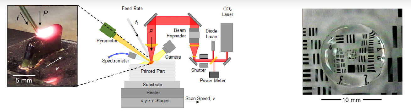
Figure 2: The Filament-Fed, Laser-Heated Process (Left) and Spherical Lens Elements (Right) [7] (Source: MS&T).
Product Innovations and Engineering (PINE, Inc.) of St. James, MO, creates innovative solutions to transform the AM industry and is partnering with Dr. E. C. Kinzel at the University of Notre Dame to further improve the FFLH process. They have shown that the FFLH process is capable of creating fully-dense, optically-transparent objects, including lenses, freely-supported structures, waveguides, and microfluidic networks.
AM for Advanced Optics
A multimaterial, precision AM optical platform would be a game changer for advanced refractive optical components based on freeform surfaces and graded index (GRIN) optics. These technologies bring increased control over the transmission and manipulation of the optical wavefront. They offer the potential for very high-performance optical designs (e.g., high image quality, wide field of view, etc.) in compact forms that would benefit platforms where size and weight are a premium, such as space-based platforms, small unmanned aerial vehicles, and the dismounted Warfighter. Optical systems based on these technologies have been historically difficult to implement with current technologies [8] and, thus, their potential has not yet been fully realized.
Conventional refractive optics with spherical and even aspherical surfaces have rotational symmetry that make them compatible with modern optical surface generating methods (e.g., SPDT). Freeform optics, which lack rotational or translational symmetry, are recently being used in developing high-quality optical systems. The spherical or low-order aspheric surfaces in conventional lenses and mirrors have a simple shape and thus are limited in their potential light-beam paths. Lenses and mirrors with more complex freeform surfaces, which are mathematically described by Zernike polynomials, are needed for many advanced applications.
Traditional 2 degrees of freedom manufacturing processes, such as grinding, polishing, and ultraprecision turning, are incapable of manufacturing freeform surfaces. Advanced methods (ion-beam figuring and five-axis diamond milling) are required to realize these surfaces. A typical lens element contributes up to 15 aberrations that must be corrected in the optical assembly by additional lens elements and aperture stops. Using a freeform shape for the surface offers an opportunity to more directly correct the limiting aberrations and reduce the number of lens elements. The additive generation of three-dimensional (3-D) optical surfaces in glass via AM is an opportunity to bolster the manufacturing and realization of freeform optics for Navy applications.
So far, we have only considered the role of optical surfaces in manipulating the optical wavefront, as the body of a homogeneous lens (ideally) does not alter its trajectory. In addition to refraction at the front and rear surfaces, GRIN optics have an internal refractive index distribution that bends light within the body of the lens. Distributing the internal GRIN profile offers the optical designer an additional degree of freedom roughly equivalent to having an additional surface.
GRIN lenses have been commercially available for some time, although the GRIN profiles have been restricted in size and shape of the index profile to those easily generated by diffusion processes. Ion-exchange diffusion through a glass rod has been used to generate purely radial gradients (e.g., SELFOC by GoFoton). Diffusion between stacked glass plates has been used to generate purely axial gradients (Gradium by LightPath). But the long time for diffusion, typically measured in months, limits the diameters of radial GRIN optics to several millimeters, with roughly parabolic index profiles. The limiting factors for the widespread adoption of GRIN in advanced optical systems are manufacturing difficulty and the constraints on the GRIN profiles that can be obtained by current methods [8].
Based on inkjet printing technology, the Volumetric Index of Refraction Gradient Optics (VIRGO) process from Voxtel, Inc., is capable of 3-D printing of lenses using two or more “inks” having different optical properties (refractive index and dispersion). This process opens the possibility to creating GRIN optics with gradients unrestrained by previous techniques. It utilizes inks comprised of optical material nanoparticles deposited onto a substrate and dispersed in a solvent voxel by voxel, layer by layer [8]. The solvent is subsequently removed, and the optic is densified under appropriate conditions to form a solid, transparent lens free of voids or pores. By overlapping multiple inks with different optical properties and allowing small-scale diffusion, optics with arbitrary, volumetric GRIN profiles can be realized, can compensate for geometric and chromatic aberrations, and can provide optical power.
If we think of GRIN from a design perspective as having an additional optical surface, 3-D GRIN represents an additional high-order, freeform surface inside the optic. Additionally, since the diffusion distances are small (~100 μm) compared to those used in other methods, the processing time is fast and scalable. Currently, the medium-scale VIRGO platform can produce organic/inorganic optics within the 1 m x 1.5 m build area, including homogenous optics, GRIN lenses, phase corrector plates, and lens array plates (as shown in Figure 3). The process is compatible with other important wavelength regimes, including UV and infrared (IR), by exploiting the appropriate materials for inks.
Voxtel and the Institute for Optics at the University of Rochester (UR) are developing an AM method to create glass gradient refractive index (GRIN) lenses. This research is an extension of Voxtel’s existing organic/inorganic VIRGO AM platform (Figure 3, left), which can simultaneously print six different inks in a 1 m x 1.5 m build area, up to 60 mm tall, at a production rate of 100 optics (25-mm diameter) per hour. The process has been used to demonstrate 4-inch-diameter GRIN lenses and phase corrector plates (Figure 3, center) as well as lenslet arrays (Figure 3, right). The UR glass melt technology will melt green state Voxtel lens samples to deliver high-performance optics.
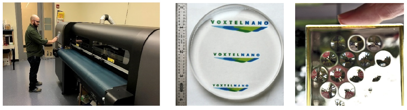
Figure 3: Voxtel’s Medium-Scale VIRGO AM Platform (Left), 4-inch-Diameter GRIN Lens and Phase Corrector Plate (Center), and Lenslet Arrays (Right) (Source: Voxtel, Inc.).
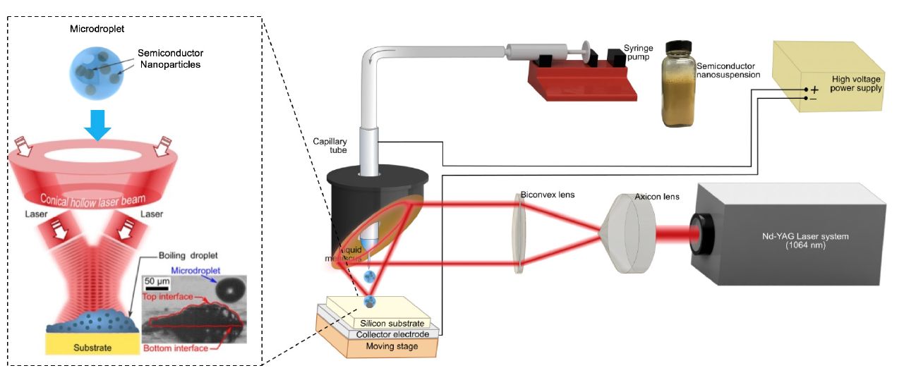
Figure 4: The NELD Process [9] (Source: CREOL, UCF).
Conclusions
Extending these optical AM methods to infrared systems, particularly those used for thermal imaging in the midwave infrared (3–5 μm) and long-wave infrared (8–12 μm) wavebands, is promising but poses another set of challenges. The materials do not have significant IR transmission beyond about 1 μm, and IR refractive materials must be adapted for use in AM. IR lenses are typically crystals (e.g., silicon, CaF2, germanium, ZnSe, ZnS, and GaAs) or chalcogenide glasses (e.g., amorphous material transmitting infrared radiation and Schott/Vitron infrared glasses series). Deposition and densification of IR crystalline nanoparticles into highquality, transparent optical ceramics is a topic of ongoing research and potentially compatible with the AM methods discussed here. Chalcogenide glasses offer a wide range of optical properties that can be controlled via the quantity of their chemical constituents [10]. However, when heated to processing temperatures, their chemistries and, hence, optical properties can change due to high vapor pressures and reactivity with water and oxygen.
Advanced infrared optics via AM, particularly IR-GRIN and freeform surfaces, can significantly reduce the size and weight of imaging and threat-warning sensors, enabling dual-band common aperture sensors and sensors with conformal apertures. In the IR wavebands, where there is little diversity in existing lens materials, chromatic aberration is a key challenge and often requires numerous lens elements. This is compounded when the system must operate in multiple wavebands.
The primary advantage of GRIN for IR is to utilize the additional degree of freedom it provides to correct chromatic aberration, thereby reducing the number of lens elements, overall system size, and shifting some of the system complexity to the lens element level for relaxed assembly tolerances and improved reliability [2, 8, 10]. To date, GRIN profiles in infrared materials have been limited to axial and hybrid axial-radial configurations due to diffusion-based fabrication techniques. A true AM approach would enable gradients with 3-D precision and advanced capabilities to platforms for all the Services.
Optical quality AM of inorganic glasses opens up new opportunities for engineering optics with volumetrically varying properties, such as GRIN lenses, as well as homogeneous lenses with advances freeform surfaces, unconstrained by the limitations of conventional lens manufacturing methods. The potential of AM for field repair of optical systems on demand will dramatically enhance the logistics and maintenance of Navy platforms and associated sensors across all Services.
Acknowledgments
In writing this article, many people have made this effort significantly easier. I want to thank Dan, my co-author, who stepped in the last minute and added significant clarity to this article and my understanding of freeform optics. I want to also thank IRFlex, Voxel, PINE, and their associated universities (UCF, UR, and Notre Dame) for their contributions; Kishan Goel (retired) in creating this STTR; Petra Branthoover for her tireless efforts in working with me to get this topic out; and Naval Air Systems Command’s SBIR/STTR Office for allowing me to expand the Navy’s portfolio in optical technology.
On a personal note, I would like to thank Jill Tyler Hurst for donating her heart to me last September. She was an amazing young woman who saved the lives of five people with her generous gifts. I want to let her loved ones know that I am eternally grateful for her gift. I want to thank the Jacksonville Mayo Clinic cardiac team for saving my life. They are truly skilled, compassionate, and caring professionals. I would also like to thank my wife, my kids, my mom, my brothers, and family and friends for getting me through this challenging period.
References
- U.S. Navy SBIR/STTR Office. “Additive Manufacturing of Inorganic Transparent Materials for Advanced Optics.” STTR topic N19B-T02, 2019.
- McCarthy, P. “Gradient-Index Materials, Design, and Metrology for Broadband Imaging Systems.” Ph.D. thesis, University of Rochester, NY, 2015.
- Willis, K., E. Brockmeyer, S. Hudson, and I. Poupyrev. “Printed Optics: 3D Printing of Embedded Optical Elements for Interactive Devices.” The 25th Annual ACM Symposium on User Interface Software and Technology, Cambridge, MA, pp. 589–598, 7–10 October 2012.
- Brockmeyer, E., I. Poupyrev, and S. Hudson. “PAPILLON: Designing Curved Display Surfaces With Printed Optics.” The 26th Annual ACM Symposium on User Interface Software and Technology, St. Andrews, Scotland, UK, pp. 457–462, 8–11 October 2013.
- Urness, A. C., K. Anderson, W. L. Wilson, and R. R. McLeod. “Arbitrary GRIN Component Fabrication in Optically Driven Diffusive Photopolymers.” Optics Express, vol. 23, pp. 264–273, 2015.
- Gissibl, T., S. Thiele, A. Herkommer, and H. Giessen. “Two-Photon Direct Laser Writing of Ultracompact Multi-Lens Objectives.” Nature Photonics, vol. 10, pp. 554–560, 2016.
- Luo, J., L. Gilbert, C. Qu, J. Wilson, D. Bristow, R. Landers, and E. Kinzel. “Wire-Fed Additive Manufacturing of Transparent Glass Parts.” Proceedings of the ASME 2015 International Manufacturing Science and Engineering Conference. Volume 1: Processing, Charlotte, NC, 8–12 June 2015, https://doi.org/10.1115/MSEC2015-9377.
- Teichman, J., J. Holzer, B. Balko, B. Fisher, and L. Buckley. “Gradient Index Optics at DARPA.” D-5027, pp. 1–69, 2013.
- Castillo-Orozco, E., R. Kumar, and A. Kar. “Laser-Induced Subwavelength Structures by Microdroplet Superlens.” Optics Express, vol. 27, pp. 8130–8142, 2019.
- Gibson, D. J., S. S. Bayya, V. Nguyen, J. S. Sanghera, G. Beadie, M. Kotov, C. McClain, and J. Vizgaitis. “Multispectral IR Optics and GRIN.” Proc. SPIE, 10998, 109980D–1–109980D–10, 2019.
Biographies
CHANDRAIKA (JOHN) SUGRIM is an electronic engineer for the U.S. Naval Air Warfare Commander Fleet Readiness Center in Jacksonville, FL. His research interests include electro-optical/IR systems design, composite laser-induced fluorescence detection, and polarization switcher optics. He has received several Engineer of the Year awards from the Navy; written manuals and publications; and presented at symposiums. He has four granted patents and five nonprovisional patent applications and was awarded a Professional Engineering license. Mr. Sugrim holds a bachelor’s degree in electrical engineering and an M.S. in physics from State University of New York at Stony Brook, an M.S. in risk management from Florida State University, and an M.S. in electrical engineering (electronic warfare) from the Navy Post Graduate School.
DANIEL GIBSON is a research scientist in the Optical Materials and Devices Branch at the U.S. Naval Research Laboratory in Washington, DC, where he has been developing infrared optical materials and fibers since 2003. He invented diffusion-based GRIN IR glass lenses and thermally-bonded IR doublet lenses that obviate the need for IR-transparent adhesives. He also developed technologies to fabricate novel infrared optical fibers, including hollow waveguides, single crystal fibers, heavy metal oxide and chalcogenide glass fibers with solid core, photonic crystal, photonic bandgap, and negative curvature structures. Dr. Gibson holds over a dozen patents on his technologies, several of which have been licensed to industry, and has served as principle investigator on multiple internally- and externally-funded research and development programs. Dr. Gibson holds a Ph.D. in ceramic and materials engineering from Rutgers University.